
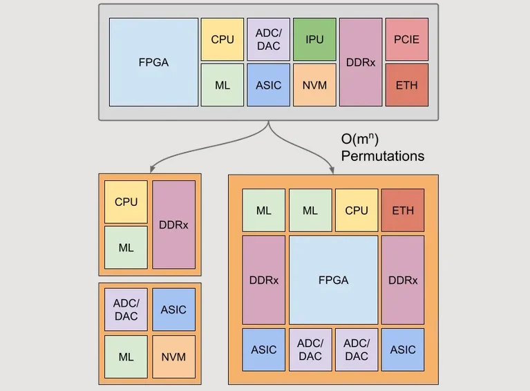
Close your eyes and visualize a future timeline. You are sitting at your workstation, utilizing a graphical user interface (GUI) to drag-and-drop standardized chiplets onto an active silicon substrate. You run your simulations, profile the performance, fine-tune the architecture, assign your package pins, and finally, press a solitary "Go" button. You sit back, perhaps sipping a coffee, waiting for your custom-designed masterpiece to arrive from the foundry.
While this sounds like the stuff of science fiction, the semiconductor industry is rapidly converging on a reality that makes this vision tangible. As we push toward the limits of physical miniaturization, a quiet revolution is taking place in the way we architect the processors of tomorrow.
The Shrinking Horizon: From Microns to Angstroms
To understand the significance of current developments, we must first appreciate the journey silicon has taken. In 1980, the design of a first-generation ASIC occurred at the 5-micron (µm) node, housing approximately 300 logic gates—a total of roughly 1,200 transistors. It was a time when every single transistor was "abused" to its maximum potential.
Over the subsequent decades, the industry defied the persistent skepticism of naysayers who claimed we would hit an insurmountable wall at every milestone: 1µm, 0.5µm, 90nm, and beyond. Today, in 2026, the industry is firmly entrenched in the 2-nanometer (nm) node, transitioning from FinFET architectures to Gate-All-Around (GAA) nanosheet transistors.
As we stare into the abyss of sub-nanometer scaling, we are entering the "Angstrom Era." The Angstrom (Å), defined as $10^-10$ meters, has long been the standard unit in chemistry and crystallography. Now, it is becoming the industry nomenclature. With IBM Research experimenting with 0.7nm (7A) technology and TSMC pushing A16 and A14 "angstrom-class" nodes, the industry is signaling that we are no longer just shrinking features—we are entering a new paradigm of materials science and quantum-limited design.
The Crisis of Complexity and the Chiplet Solution
As transistor counts reach the tens of billions per die, we have hit the "reticle limit"—the physical maximum size that lithography machines can print in a single exposure. The industry’s answer to this physical constraint is the move toward heterogeneous integration, or chiplets.
Instead of a monolithic, humongous die, companies like AMD, Intel, and Nvidia have pivoted to partitioning designs across multiple smaller silicon pieces. By combining high-speed I/O on lower-cost processes with high-performance compute chiplets on cutting-edge nodes, these giants have maintained the pace of Moore’s Law. However, this has historically been an "insider’s game." Only companies with massive resources, entire ecosystems, and vertical control over their packaging can afford to navigate the complexities of multi-die integration.
Zero ASIC: A New Architectural Approach
This is where Zero ASIC, led by CEO Andreas Olofsson, enters the frame. The company is not merely proposing another interface standard; it is rethinking the fundamental "floor" of chiplet design.
Traditional multi-die systems rely on passive silicon interposers—essentially "dumb" bridges that move signals between chips. Zero ASIC has introduced the concept of an active silicon substrate. This substrate functions as a chip in its own right, embedding a Network-on-Chip (NoC), buffers, and registers directly into the foundation that supports the chiplets.
"We have four billion transistors on our substrate," Olofsson noted during a recent discussion. This active fabric allows for a level of modularity that was previously impossible. Among their key innovations is the "Platypus" eFPGA technology. Much like RISC-V revolutionized instruction set architectures by providing an open standard, Platypus offers an open eFPGA architecture. It allows designers to treat configurable logic as a standard, reusable building block, fabricated across various foundries and process nodes.
Eliminating the Manual Bottleneck: The Package Compiler
While Zero ASIC has successfully taped out its first prototype silicon—an engineering vehicle containing the active fabric, a Platypus FPGA chiplet, and a quad-core RISC-V CPU—the most significant news involves their recent software advancement.

Previously, the design flow was hampered by the final, manual stage of packaging. In a traditional workflow, an engineer hands a spreadsheet to an OSAT (Outsourced Semiconductor Assembly and Test) partner, waits for a manual layout, reviews it, and undergoes a tedious, error-prone cycle of revisions.
Zero ASIC has now unveiled a "Package Compiler." This software takes a completed chiplet design and a target package style, then automatically generates a design-rule-clean package layout. It routes connections from the chip bumps directly to the external BGA pins without human intervention. By automating this, Zero ASIC has removed the final major obstacle between "drag-and-drop" design and physical reality.
Implications: The Democratization of Custom Silicon
The implications of this shift are profound. For decades, the design of a custom SoC (System on Chip) has been the exclusive domain of companies with hundreds of millions of dollars and teams of specialized engineers.
If the "Compile-to-Silicon" vision matures, the barrier to entry could collapse. Small startups, research labs, and academic institutions could theoretically synthesize a complex, multi-die system using a library of off-the-shelf chiplets.
The Path Forward
However, the road to this "Go button" future is still under construction. As Olofsson acknowledges, the current prototype phase is just the beginning. To reach widespread commercial viability, Zero ASIC must expand its library of standard chiplets to include critical infrastructure components, such as high-performance DDR controllers. Olofsson estimates that approximately $25 million in additional investment is required to reach a "minimum viable library" that would satisfy the broader market.
The company is currently looking for partners to help build this ecosystem. The goal is to move beyond proprietary, isolated solutions and toward a truly composable, interoperable silicon marketplace.
A Vision 15 Years in the Making
Andreas Olofsson’s pursuit of this vision is not a recent whim; it spans over fifteen years of industry tenure. From his work at Adapteva to the Parallella supercomputer project, Olofsson has consistently advocated for making high-performance computing accessible to the masses.
"Each step has moved us closer to the same destination," Olofsson remarked. The ultimate goal remains the same: to make custom silicon something that an ordinary engineering team can create without needing an army of specialists.
Whether Zero ASIC is the company that finally achieves this, or if they are simply setting the standard for those who will follow, one thing is certain: the era of the monolithic, one-size-fits-all processor is drawing to a close. We are moving toward a future where silicon design is no longer a dark art practiced by the few, but a composable, automated, and accessible utility for the many.
As we stand on the precipice of the Angstrom Era, the ability to rapidly iterate and customize silicon will likely define the next generation of technological innovation. For the engineers and architects watching this space, the "Go" button is closer than it has ever been.