In the rapidly evolving landscape of System-on-Chip (SoC) design and multi-die system (MDS) architectures, there is a prevailing sentiment that we are constantly reinventing the wheel. However, as the philosopher George Santayana famously noted, “Those who cannot remember the past are condemned to repeat it.” In the realm of high-performance computing and semiconductor engineering, this axiom takes on a more optimistic, specialized hue: those who succeed in learning from history’s successes are destined to replicate them.
The fundamental challenge of computing, spanning over sixty years, has remained remarkably constant: how to facilitate efficient, high-bandwidth, and low-latency communication between an ever-increasing number of functional entities. Whether those entities are logic blocks inside a monolithic chip or autonomous chiplets in a multi-die package, the architectural patterns of the past provide the blueprint for the AI-driven future.
The Chronology of Connectivity: From Buses to NoCs
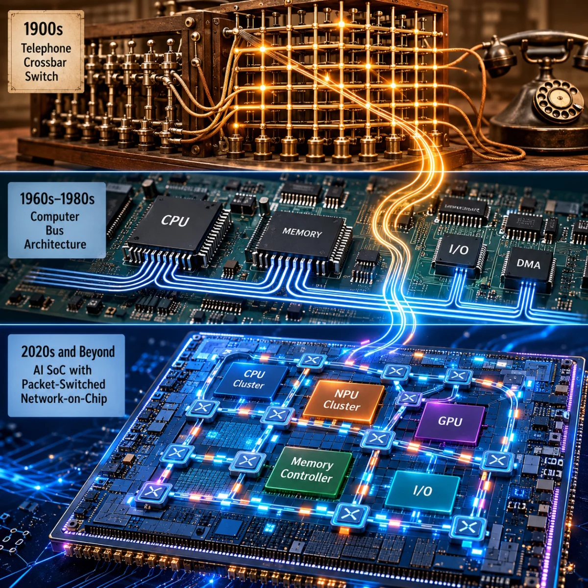
To understand where we are going, we must trace the cyclical evolution of communication architectures. This progression has played out across three distinct domains: communication within a single computer, communication between separate computers, and, most recently, communication within highly complex SoCs.
The Era of the Shared Bus
In the nascent stages of computing, simplicity was paramount. Systems were composed of a Central Processing Unit (CPU), random-access memory (RAM), and a limited array of peripherals. The industry standard was the "shared bus"—a singular collection of wires acting as a common thoroughfare. While elegant and cost-effective, the shared bus suffered from a critical limitation: it was a single-conversation medium. Only one master could control the bus at any given time, creating a massive performance bottleneck as processor speeds outpaced memory access and I/O throughput.
The Rise of the Crossbar Switch
As performance demands escalated, engineers moved toward crossbar switches. By providing dedicated, non-blocking paths between multiple masters and slaves, crossbars allowed for simultaneous transactions. A CPU could fetch instructions from memory while a Direct Memory Access (DMA) controller moved data from storage, effectively multiplying throughput. Yet, crossbars faced a scalability wall; the geometric increase in wiring complexity, routing congestion, and silicon area made them unsustainable for the massive integration of modern SoCs.

The Shift to Packet-Switched Networks
Borrowing from the networking world, the industry eventually transitioned to packet-switched interconnects. By abandoning the requirement for dedicated, permanent paths, designers could package data into packets routed through distributed switches. Technologies such as PCI Express, while physically serial, are architecturally packet-switched systems. This transition mirrored the evolution of wide-area computer networks, where the need to connect thousands of nodes rendered dedicated circuit-switching impractical, favoring the dynamic, packet-based efficiency of the Internet.
Architectural Convergence: The SoC and the NoC
The modern SoC has effectively become a microcosm of the global network. As SoCs grew to encompass dozens of processor clusters, graphics engines, and DSPs, the shared bus and the crossbar were pushed to their limits. This birthed the Network-on-Chip (NoC).
The NoC is perhaps the most prominent example of an engineering success from the past being repurposed. By implementing a distributed network of on-chip routers, designers can support hundreds of intellectual property (IP) blocks. This architecture keeps wiring complexity under control while providing the high-bandwidth backbone necessary for modern computing. It is the evolution of the network switch brought down to the nanometer scale.
The AI Disruption: A New Paradigm for Data Flow
The arrival of Artificial Intelligence (AI) and Machine Learning (ML) has fundamentally altered the communication landscape. Traditional SoCs dealt with general-purpose traffic—balanced workloads between CPUs and peripherals. AI, however, introduces Neural Processing Units (NPUs) and AI accelerators that operate on massive, streaming datasets—tensors, feature maps, and model weights—that dwarf the control-plane data of a standard CPU.
The Coherent vs. Non-Coherent Split
According to industry experts, including those at Arteris, we are witnessing an "architectural split." The old philosophy of a single, unified interconnect is giving way to a dual-layered approach:

- The Coherent Backbone: Used for control structures, pointers, and semaphores, where data integrity and cache coherency are paramount.
- The Non-Coherent Streaming Fabric: Dedicated to the massive, "bulk" movement of AI data that does not require cache coherency, thereby reducing unnecessary overhead.
This duality allows for a highly efficient "conductor-and-backstage" dynamic. The coherent NoC ensures that the CPU and accelerators remain in sync, acting as the orchestra conductor, while the non-coherent NoCs move the heavy, high-volume data behind the scenes, ensuring the system remains responsive and energy-efficient.
Official Industry Perspectives: The Arteris Approach
In recent discussions with leaders at Arteris, the strategy for addressing these AI-specific demands has become clear. The company is currently deploying two distinct yet complementary IP solutions: Ncore and FlexGen.
- Ncore: This IP serves as the coherent backbone. It ensures that data remains consistent across the SoC, which is vital when multiple processors and accelerators need to access the same memory regions.
- FlexGen: This represents the next leap in interconnect automation. Utilizing AI-assisted optimization, FlexGen generates non-coherent NoCs that are specifically tuned for streaming traffic. By minimizing wire length and latency, it significantly reduces the power footprint of the SoC—a critical metric in both mobile and data-center AI hardware.
As Ashley Stevens of Arteris points out, the coherent NoC itself is not static. In smaller devices, it may function as a centralized hub. However, as chips scale to the "AI monster" level, the coherency fabric is increasingly evolving into a distributed mesh, mirroring the very network topologies that revolutionized the global internet decades ago.
Implications for Future Multi-Die Systems (MDS)
The final frontier for interconnect technology is the multi-die system (MDS). As we hit the physical limits of reticle sizes on a single piece of silicon, the industry is moving toward chiplets.
The architectural principles that governed the transition from buses to NoCs are now being stretched across the interposer. From the perspective of the software, an MDS must appear as a single, unified, coherent system. This requires the same sophisticated NoC strategies—coherent backbones coupled with high-speed streaming fabrics—to be extended between dies.

Conclusion: The Endurance of Good Engineering
The history of interconnect technology is not a story of constant reinvention, but one of constant refinement. We have moved from simple wires to sophisticated, AI-optimized, distributed meshes. Every time we encounter a bottleneck, we reach into the toolbox of history—finding that the solutions implemented for telephone exchanges or mainframe networks are, with some modification, the exact answers needed for the next generation of neural processing chips.
As we look toward the future of 3D-stacked silicon and massive multi-die AI clusters, one thing remains certain: the engineers who recognize these recurring patterns will be the ones to lead the next era of technological progress. Good ideas, it seems, truly never die; they simply wait for the scale of the problem to catch up to their potential. For the engineering community, this is not just a lesson in history—it is a roadmap for the future.